


|
Doing random things over at http://musteat.org
|


By Mark Brand, Google Project Zero
Introduction
It's finally time for me to fulfill a long-standing promise. Since I first heard about ARM's Memory Tagging Extensions, I've said (to far too many people at this point to be able to back out…) that I'd immediately switch to the first available device that supported this feature. It's been a long wait (since late 2017) but with the release of the new Pixel 8 / Pixel 8 Pro handsets, there's finally a production handset that allows you to enable MTE!
The ability of MTE to detect memory corruption exploitation at the first dangerous access is a significant improvement in diagnostic and potential security effectiveness. The availability of MTE on a production handset for the first time is a big step forward, and I think there's real potential to use this technology to make 0-day harder.
I've been running my Pixel 8 with MTE enabled since release day, and so far I haven't found any issues with any of the applications I use on a daily basis1, or any noticeable performance issues.
Currently, MTE is only available on the Pixel as a developer option, intended for app developers to test their apps using MTE, but we can configure it to default to synchronous mode for all2 apps and native user mode binaries. This can be done on a stock image, without bootloader unlocking or rooting required - just a couple of debugger commands. We'll do that now, but first:
Disclaimer
This is absolutely not a supported device configuration; and it's highly likely that you'll encounter issues with at least some applications crashing or failing to run correctly with MTE if you set your device up in this way.
This is how I've configured my personal Pixel 8, and so far I've not experienced any issues, but this was somewhat of a surprise to me, and I'm still waiting to see what the first app that simply won't work at all will be...
Enabling MTE on Pixel 8/Pixel 8 Pro
Enabling MTE on an Android device requires the bootloader to reserve a portion of the device memory for storing tags. This means that there are two separate places where MTE needs to be enabled - first we need to configure the bootloader to enable it, and then we need to configure the system to use it in applications.
First we need follow the Android instructions to enable developer mode and USB debugging on the device:

Now we need to connect our phone to a trusted computer that has the Android debugging tools installed on it - I'm using my linux workstation:
markbrand@markbrand$ adb devices -l
List of devices attached
XXXXXXXXXXXXXX device usb:3-3 product:shiba model:Pixel_8 device:shiba transport_id:5
markbrand@markbrand$ adb shell
shiba:/ $ setprop arm64.memtag.bootctl memtag
shiba:/ $ setprop persist.arm64.memtag.default sync
shiba:/ $ setprop persist.arm64.memtag.app_default sync
shiba:/ $ reboot
These commands are doing a couple of things - first, we're configuring the bootloader to enable MTE at boot. The second command sets the default MTE mode for native executables running on the device, and the third command sets the default MTE mode for apps. An app developer can enable MTE by using the manifest, but this system property sets the default MTE mode for apps, effectively making it opt-out instead of opt-in.
While on the topic of apps opting-out, it's worth noting that Chrome doesn't use the system allocator for most allocations, and instead uses PartitionAlloc. There is experimental MTE support under development, which can be enabled with some additional steps3. Unfortunately this currently requires setting a command-line flag which involves some security tradeoffs. We expect that Chrome will add an easier way to enable MTE support without these problems in the near future.
If we look at all of the system properties, we can see that there are a few additional properties that are related to memory tagging:
shiba:/ $ getprop | grep memtag
[arm64.memtag.bootctl]: [memtag]
[persist.arm64.memtag.app.com.android.nfc]: [off]
[persist.arm64.memtag.app.com.android.se]: [off]
[persist.arm64.memtag.app.com.google.android.bluetooth]: [off]
[persist.arm64.memtag.app_default]: [sync]
[persist.arm64.memtag.default]: [sync]
[persist.arm64.memtag.system_server]: [off]
[ro.arm64.memtag.bootctl_supported]: [1]
There are unfortunately some default exclusions which we can't overwrite - the protections on system properties mean that we can't currently enable MTE for a few components in a normal production build - these exceptions are system_server and applications related to nfc, the secure element and bluetooth.
We wanted to make sure that these commands work, so we'll do that now. We'll first check whether it's working for native executables:
shiba:/ $ cat /proc/self/smaps | grep mt
VmFlags: rd wr mr mw me ac mt
VmFlags: rd wr mr mw me ac mt
VmFlags: rd wr mr mw me ac mt
VmFlags: rd wr mr mw me ac mt
VmFlags: rd wr mr mw me ac mt
VmFlags: rd wr mr mw me ac mt
VmFlags: rd wr mr mw me ac mt
765bff1000-765c011000 r--s 00000000 00:12 97 /dev/__properties__/u:object_r:arm64_memtag_prop:s0
We can see that our cat process has mappings with the mt bit set, so MTE has been enabled for the process.
Now in order to check that an app without any manifest setting has picked up this, we added a little bit of code to an empty JNI project to trigger a use-after-free bug:
extern "C" JNIEXPORT jstring JNICALL
Java_com_example_mtetestapplication_MainActivity_stringFromJNI(
JNIEnv* env,
jobject /* this */) {
char* ptr = strdup("test string");
free(ptr);
// Use-after-free when ptr is accessed below.
return env->NewStringUTF(ptr);
}
Without MTE, it's unlikely that the application would crash running this code. I also made sure that the application manifest does not set MTE, so it will inherit the default. When we launch the application we will see whether it crashes, and whether the crash is caused by an MTE check failure!

Looking at the logcat output we can see that the cause of the crash was a synchronous MTE tag check failure (SEGV_MTESERR).
DEBUG : *** *** *** *** *** *** *** *** *** *** *** *** *** *** *** ***
DEBUG : Build fingerprint: 'google/shiba/shiba:14/UD1A.230803.041/10808477:user/release-keys'
DEBUG : Revision: 'MP1.0'
DEBUG : ABI: 'arm64'
DEBUG : Timestamp: 2023-10-24 16:56:32.092532886+0200
DEBUG : Process uptime: 2s
DEBUG : Cmdline: com.example.mtetestapplication
DEBUG : pid: 24147, tid: 24147, name: testapplication >>> com.example.mtetestapplication <<<
DEBUG : uid: 10292
DEBUG : tagged_addr_ctrl: 000000000007fff3 (PR_TAGGED_ADDR_ENABLE, PR_MTE_TCF_SYNC, mask 0xfffe)
DEBUG : pac_enabled_keys: 000000000000000f (PR_PAC_APIAKEY, PR_PAC_APIBKEY, PR_PAC_APDAKEY, PR_PAC_APDBKEY)
DEBUG : signal 11 (SIGSEGV), code 9 (SEGV_MTESERR), fault addr 0x0b000072afa9f790
DEBUG : x0 0000000000000001 x1 0000007fe384c2e0 x2 0000000000000075 x3 00000072aae969ac
DEBUG : x4 0000007fe384c308 x5 0000000000000004 x6 7274732074736574 x7 00676e6972747320
DEBUG : x8 0000000000000020 x9 00000072ab1867e0 x10 000000000000050c x11 00000072aaed0af4
DEBUG : x12 00000072aaed0ca8 x13 31106e3dee7fb177 x14 ffffffffffffffff x15 00000000ebad6a89
DEBUG : x16 0000000000000001 x17 000000722ff047b8 x18 00000075740fe000 x19 0000007fe384c2d0
DEBUG : x20 0000007fe384c308 x21 00000072aae969ac x22 0000007fe384c2e0 x23 070000741fa897b0
DEBUG : x24 0b000072afa9f790 x25 00000072aaed0c18 x26 0000000000000001 x27 000000754a5fae40
DEBUG : x28 0000007573c00000 x29 0000007fe384c260
DEBUG : lr 00000072ab35e7ac sp 0000007fe384be30 pc 00000072ab1867ec pst 0000000080001000
DEBUG : 98 total frames
DEBUG : backtrace:
DEBUG : #00 pc 00000000003867ec /apex/com.android.art/lib64/libart.so (art::(anonymous namespace)::ScopedCheck::Check(art::ScopedObjectAccess&, bool, char const*, art::(anonymous namespace)::JniValueType*) (.__uniq.99033978352804627313491551960229047428)+1636) (BuildId: a5fcf27f4a71b07dff05c648ad58e3cd)
DEBUG : #01 pc 000000000055e7a8 /apex/com.android.art/lib64/libart.so (art::(anonymous namespace)::CheckJNI::NewStringUTF(_JNIEnv*, char const*) (.__uniq.99033978352804627313491551960229047428.llvm.6178811259984417487)+160) (BuildId: a5fcf27f4a71b07dff05c648ad58e3cd)
DEBUG : #02 pc 00000000000017dc /data/app/~~lgGoAt3gB6oojf3IWXi-KQ==/com.example.mtetestapplication-k4Yl4oMx9PEbfuvTEkjqFg==/base.apk!libmtetestapplication.so (offset 0x1000) (_JNIEnv::NewStringUTF(char const*)+36) (BuildId: f60a9970a8a46ff7949a5c8e41d0ece51e47d82c)
...
DEBUG : Note: multiple potential causes for this crash were detected, listing them in decreasing order of likelihood.
DEBUG : Cause: [MTE]: Use After Free, 0 bytes into a 12-byte allocation at 0x72afa9f790
DEBUG : deallocated by thread 24147:
DEBUG : #00 pc 000000000005e800 /apex/com.android.runtime/lib64/bionic/libc.so (scudo::Allocator<scudo::AndroidConfig, &(scudo_malloc_postinit)>::quarantineOrDeallocateChunk(scudo::Options, void*, scudo::Chunk::UnpackedHeader*, unsigned long)+496) (BuildId: a017f07431ff6692304a0cae225962fb)
DEBUG : #01 pc 0000000000057ba4 /apex/com.android.runtime/lib64/bionic/libc.so (scudo::Allocator<scudo::AndroidConfig, &(scudo_malloc_postinit)>::deallocate(void*, scudo::Chunk::Origin, unsigned long, unsigned long)+212) (BuildId: a017f07431ff6692304a0cae225962fb)
DEBUG : #02 pc 000000000000179c /data/app/~~lgGoAt3gB6oojf3IWXi-KQ==/com.example.mtetestapplication-k4Yl4oMx9PEbfuvTEkjqFg==/base.apk!libmtetestapplication.so (offset 0x1000) (Java_com_example_mtetestapplication_MainActivity_stringFromJNI+40) (BuildId: f60a9970a8a46ff7949a5c8e41d0ece51e47d82c)
If you just want to check that MTE has been enabled in the bootloader, there's an application on the Play Store from Google's Dynamic Tools team, which you can also use (this app enables MTE in async mode in the manifest, which is why you see below that it's not running in sync mode on all cores):

At this point, we can go back into the developer settings and disable USB debugging, since we don't want that enabled for normal day-to-day usage. We do need to leave the developer mode toggle on, since disabling that will turn off MTE again entirely on the next reboot.
Conclusion
The Pixel 8 with synchronous-MTE enabled is at least subjectively a performance and battery-life upgrade over my previous phone.
I think this is a huge improvement for the general security of the device - many zero-click attack surfaces involve large amounts of unsafe C/C++ code, whether that's WebRTC for calling, or one of the many media or image file parsing libraries. MTE is not a silver bullet for memory safety - but the release of the first production device with the ability to run almost all user-mode applications with synchronous-MTE is a huge step forward, and something that's worth celebrating!
1 On a team member's device, a single MTE detection of a use-after-free bug happened last week. This resulted in a crash that wasn't noticed at the time, but which we later found when looking through the saved crash reports on their device. Because the alloc and free stacktraces of the allocation were recorded, we were able to quickly figure out the bug and report it to the application developers - the bug in this case was caused by user gesture input, and doesn't really have security impact, but it already illustrates some of the advantages of MTE.
2 Except for se (secure element), bluetooth, nfc, and the system server, due to these system apps explicitly setting their individual system properties to 'off' in the Pixel system image.
3 Enabling MTE in Chrome requires setting multiple command line flags, which on a non-rooted Android device requires configuring Chrome to load the command line flags from a file in /data/local/tmp. This is potentially unsafe, so we'd not suggest doing this, but if you'd like to experiment on a test device or for fuzzing, the following commands will allow you to run Chrome with MTE enabled:
markbrand@markbrand:~$ adb shell
shiba:/ $ umask 022
shiba:/ $ echo "_ --enable-features=PartitionAllocMemoryTagging:enabled-processes/all-processes/memtag-mode/sync --disable-features=PartitionAllocPermissiveMte,KillPartitionAllocMemoryTagging" > /data/local/tmp/chrome-command-line
shiba:/ $ ls -la /data/local/tmp/chrome-command-line
-rw-r--r-- 1 shell shell 176 2023-10-25 19:14 /data/local/tmp/chrome-command-line
Having run these commands, we need to configure Chrome to read the command line file; this can be done by opening Chrome, browsing to chrome://flags#enable-command-line-on-non-rooted-devices, and setting the highlighted flag to "Enabled".
Note that unfortunately this only applies to webpages viewed using the Chrome app, and not to other Chromium-based browsers or non-browser apps that use the Chromium based Android WebView to implement their rendering.


Cryptography tells us how to make a chain of trust rooted in special-purpose chips known as secure elements. But how do we come to trust our secure elements? I have been searching for solutions to this thorny supply chain problem. Ideally, one can directly inspect the construction of a chip, but any viable inspection method must verify the construction of silicon chips after they have been integrated into finished products, without having to unmount or destroy the chips (“in situ“). The method should also ideally be cheap and simple enough for end users to access.
This post introduces a technique I call “Infra-Red, In Situ” (IRIS) inspection. It is founded on two insights: first, that silicon is transparent to infra-red light; second, that a digital camera can be modified to “see” in infra-red, thus effectively “seeing through” silicon chips. We can use these insights to inspect an increasingly popular family of chip packages known as Wafer Level Chip Scale Packages (WLCSPs) by shining infrared light through the back side of the package and detecting reflections from the lowest layers of metal using a digital camera. This technique works even after the chip has been assembled into a finished product. However, the resolution of the imaging method is limited to micron-scale features.
This post will start by briefly reviewing why silicon inspection is important, as well as some current methods for inspecting silicon. Then, I will go into the IRIS inspection method, giving background on the theory of operation while disclosing methods and initial results. Finally, I’ll contextualize the technique and discuss methods for closing the gap between micron-scale feature inspection and the nanometer-scale features found in today’s chip fabrication technology.
DOI: 10.48550/arXiv.2303.07406
Side Note on Trust Models
Many assume the point of trustable hardware is so that a third party can control what you do with your computer – like the secure enclave in an iPhone or a TPM in a PC. In this model, users delegate trust to vendors, and vendors do not trust users with key material: anti-tamper measures take priority over inspectability.
Readers who make this assumption would be confused by a trust method that involves open source and user inspections. To be clear, the threat model in this post assumes no third parties can be trusted, especially not the vendors. The IRIS method is for users who want to be empowered to manage their own key material. I acknowledge this is an increasingly minority position.
Why Inspect Chips?
The problem boils down to chips being literal black boxes with nothing but the label on the outside to identify them.
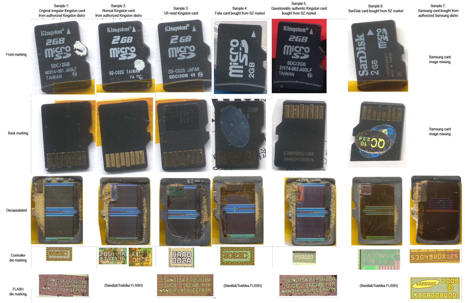
For example, above is a study I performed surveying the construction of microSD cards in an effort to trace down the root cause of a failed lot of products. Although every microSD card ostensibly advertised the same product and brand (Kingston 2GB), a decap study (where the exterior black epoxy is dissolved using a strong acid revealing the internal chips while destroying the card) revealed a great diversity in internal construction and suspected ghost runs. The take-away is that labels can’t be trusted; if you have a high-trust situation, something more is needed to establish a device’s internal construction than the exterior markings on a chip’s package.
What Are Some Existing Options for Inspecting Chips?
There are many options for inspecting the construction of chips; however, all of them suffer from a “Time Of Check versus Time Of Use” (TOCTOU) problem. In other words, none of these techniques are in situ. They must be performed either on samples of chips that are merely representative of the exact device in your possession, or they must be done at remote facilities such that the sample passes through many stranger’s hands before returning to your possession.

Scanning Electron Microscopy (SEM), exemplified above, is a popular method for inspecting chips (image credit: tmbinc). The technique can produce highly detailed images of even the latest nanometer-scale transistors. However, the technique is destructive: it can only probe the surface of a material. In order to image transistors one has to remove (through etching or polishing) the overlying layers of metal. Thus, the technique is not suitable for in situ inspection.
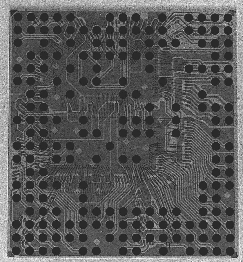
X-rays, exemplified in the above image of a MTK6260DA , are capable of non-destructive in situ inspection; anyone who has traveled by air is familiar with the applicability of X-rays to detect foreign objects inside locked suitcases. However, silicon is nearly transparent to the types of X-rays used in security checkpoints, making it less suitable for establishing the contents of a chip package. It can identify the size of a die and the position of bond wires, but it can’t establish much about the pattern of transistors on a die.
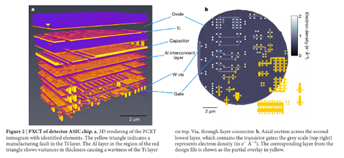
X-Ray Ptychography is a technique using high energy X-rays that can non-destructively establish the pattern of transistors on a chip. The image above is an example of a high-resolution 3D image generated by the technique, as disclosed in this Nature paper.

It is a very powerful technique, but unfortunately it requires a light source the size of a building, such as the Swiss Light Source (SLS) (donut-shaped building in the image above), of which there are few in the world. While it is a powerful method, it is impractical for inspecting every end user device. It also suffers from the TOCTOU problem in that your sample has to be mailed to the SLS and then mailed back to you. So, unless you hand-carried the sample to and from the SLS, your device is now additionally subject to “evil courier” attacks.
Optical microscopy – with a simple benchtop microscope, similar to those found in grade-school classrooms around the world – is also a noteworthy tool for inspecting chips that is easier to access than the SLS. Visible light can be a useful tool for checking the construction of a chip, if the chip itself has not been obscured with an opaque, over-molded plastic shell.
Fortunately, in the world of chip packaging, it has become increasingly popular to package chips with no overmolded plastic. The downside of exposing delicate silicon chips to possible mechanical abuse is offset by improved thermal performance, better electrical characteristics, smaller footprints, as well as typically lower costs when compared to overmolding. Because of its compelling advantages this style of packaging is ubiquitous in mobile devices. A common form of this package is known as the “Wafer Level Chip Scale Package” (WLCSP), and it can be optically inspected prior to assembly.
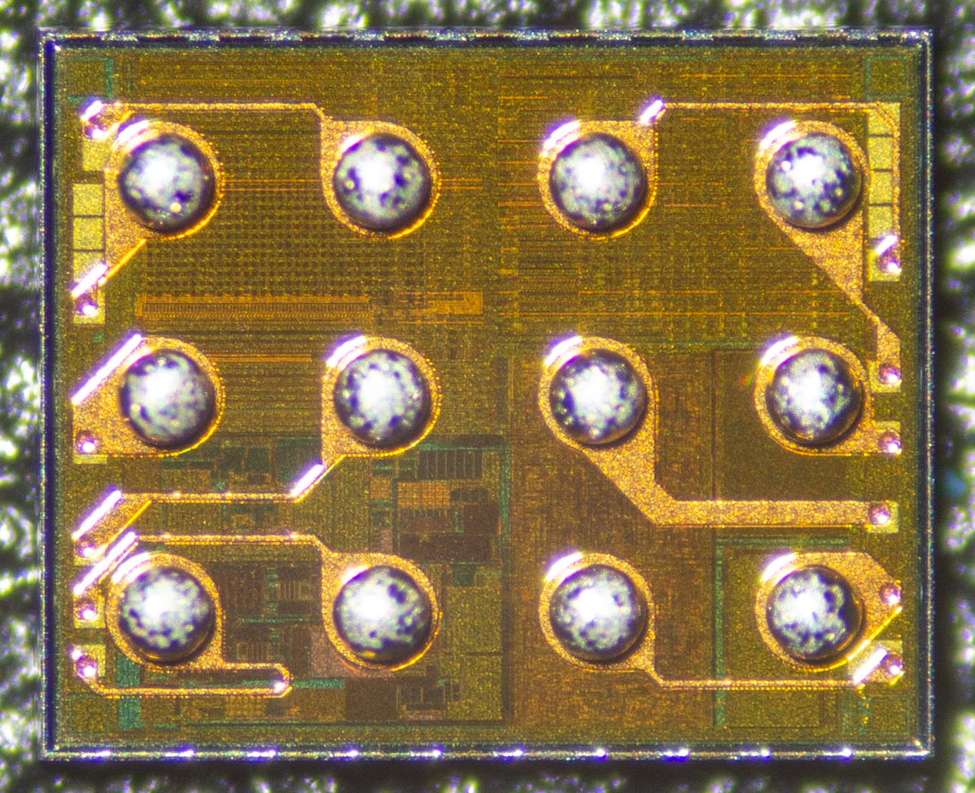
Above is an example of such a package viewed with an optical microscope, prior to attachment to a circuit board. In this image, the back side of the wafer is facing away from us, and the front side is dotted with 12 large silvery circles that are solder balls. The spacing of these solder balls is just 0.5mm – this chip would easily fit on your pinky nail.
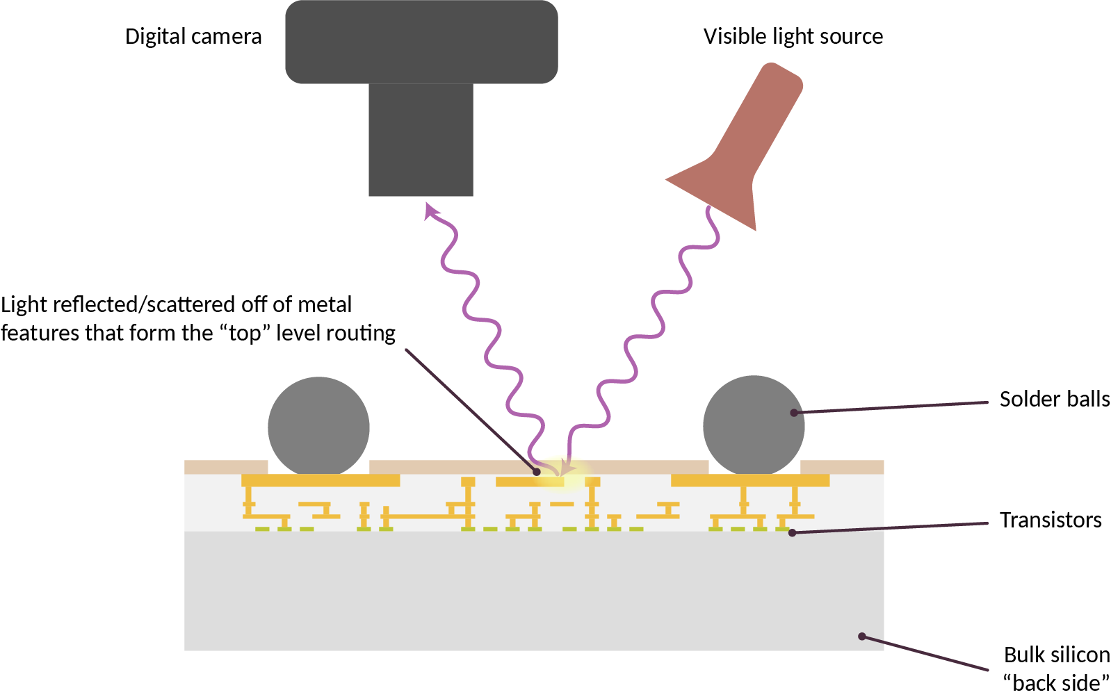
The imaged chip is laying on its back, with the camera and light source reflecting light off of the top level routing features of the chip, as illustrated in the cross-section diagram above. Oftentimes these top level metal features take the form of a regular waffle-like grid. This grid of metal distributes power for the underlying logic, obscuring it from direct optical inspection.
Note that the terms “front” and “back” are taken from the perspective of the chip’s designer; thus, once the solder balls are attached to the circuit board, the “front side” with all the circuitry is obscured, and the plain silvery or sometimes paint-coated “back side” is what’s visible.
As a result, these chip packages look like opaque silvery squares, as demonstrated in the image above. Therefore front-side optical microscopy is not suitable for in situ inspection, as the chip must be removed from the board in order to see the interesting bits on the front side of the chip.
The IRIS Inspection Method
The Infra-Red, In Situ (IRIS) inspection method is capable of seeing through a chip already attached to a circuit board, and non-destructively imaging the construction of a chip’s logic.
Here’s a GIF that shows what it means in practice:
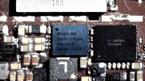
We start with an image of a WLCSP chip in visible light, assembled to a finished PCB (in this case, an iPhone motherboard). The scene is then flooded with 1070 nm infrared light, causing it to take on a purplish hue. I then turn off the visible light, leaving only the infrared light on. The internal structure of the chip comes into focus as we adjust the lens. Finally, the IR illuminator is moved around to show how the chip’s internal metal layers glint with light reflected through the body of the silicon.
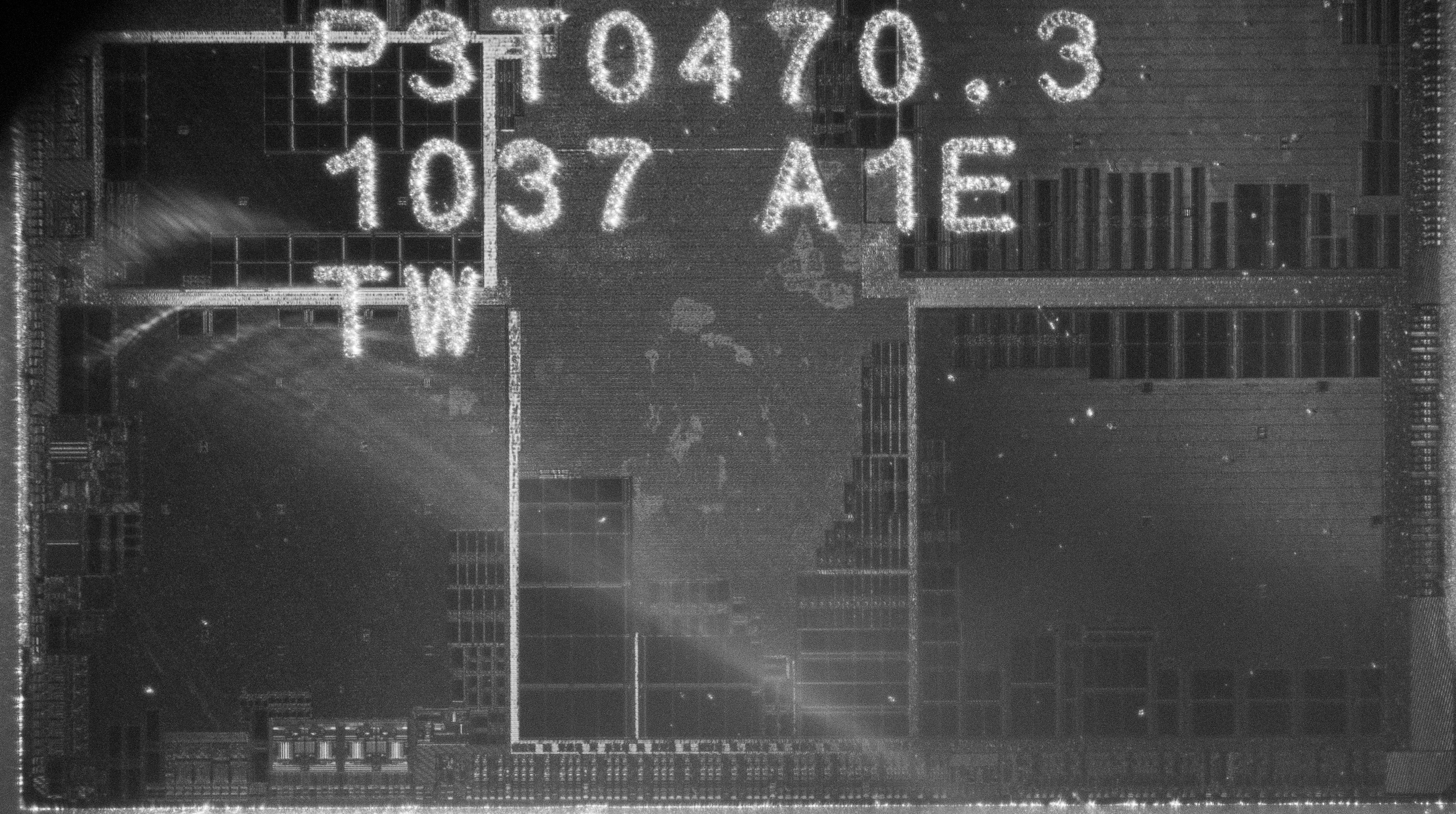
Here is a still image of the above chip imaged in infra-red, at a higher resolution:

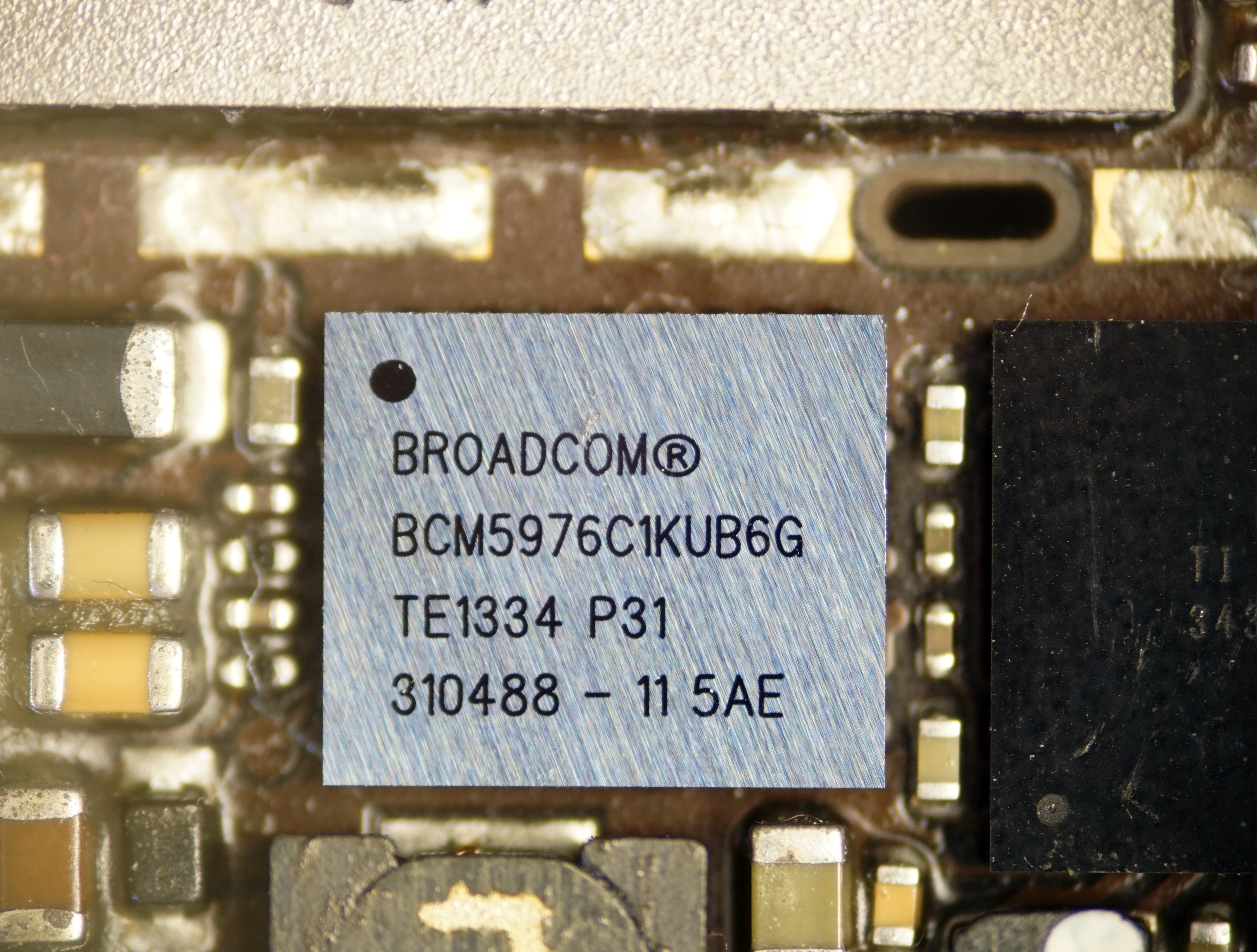
The chip is the BCM5976, a capacitive touchscreen driver for older models of iPhones. The image reveals the macro-scopic structure of the chip, with multiple channels of data converters on the top right and right edge, along with several arrays of non-volatile memory and RAM along the lower half. From the top left extending to the center is a sea of standard cell logic, which has a “texture” based on the routing density of the metal layers. Remember, we’re looking through the backside of the chip, so the metal layer we’re seeing is mostly M1 (the metal connecting directly to the transistors). The diagonal artifacts apparent through the standard cell region are due to a slight surface texture left over from wafer processing.
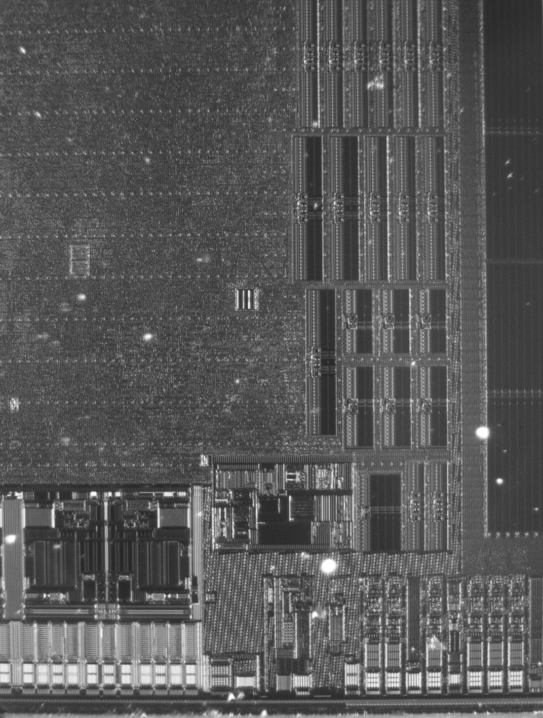
Below is the region in the pink rectangle at a higher magnification (click on the image to open a full-resolution version):
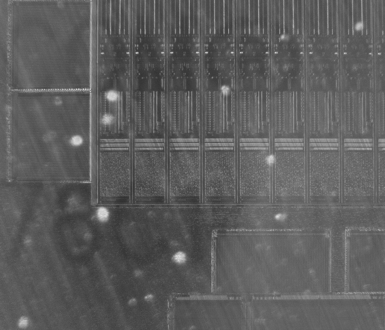
The magnified region demonstrates the imaging of meso-scopic structures, such as the row and structure column of memory macros and details of the data converters.
The larger image is 2330 pixels wide, while the chip is 3.9 mm wide: so each pixel corresponds to about 1.67 micron. To put that in perspective, if the chip were fabricated in 28 nm that would correspond to a “9-track” standard cell logic gate being 0.8 microns tall (based on data from Wikichip). Thus while these images cannot precisely resolve individual logic gates, the overall brightness of a region will bear a correlation to the type and density of logic gate used. Also please remember that IRIS is still at the “proof of concept” stage, and there are many things I’m working on to improve the image quality and fidelity.
Here’s another demo of the technique in action, on a different iPhone motherboard:
How Does It Work?
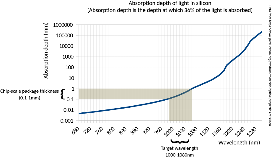
Silicon goes from opaque to transparent in the range of 1000 nm to 1100 nm (shaded band in the illustration below). Above 1100 nm, it’s as transparent as a pane of glass; below 1000 nm, it rapidly becomes more opaque than the darkest sunglasses.
Meanwhile, silicon-based image sensors retain some sensitivity in the near-to-short wave IR bands, as illustrated below.
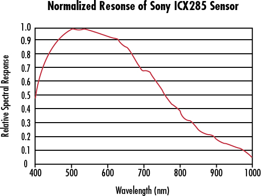
Between these two curves, there is a “sweet spot” where standard CMOS sensors retain some sensitivity to short-wave infrared, yet silicon is transparent enough that sufficient light passes through the layer of bulk silicon that forms the back side of a WLCSP package to do reflected-light imaging. More concretely, at 1000 nm a CMOS sensor might have 0.1x its peak sensitivity, and a 0.3 mm thick piece of silicon may pass about 10% of the incident light – so overall we are talking about a ~100x reduction in signal intensity compared to visible light operations. While this reduction is non-trivial, it is surmountable with a combination of a more intense light source and a longer exposure time (on the order of several seconds).
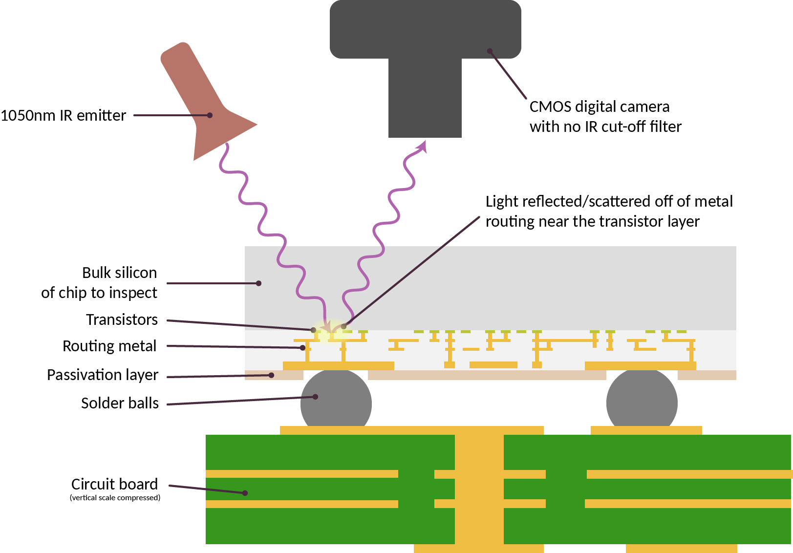
Above is a cross-section schematic of the IRIS inspection setup. Here, the sample for inspection is already attached to a circuit board and we are shining light through the back side of the silicon chip. The light reflects off of the layers of metal closest to the transistors, and is imaged using a camera. Conceptually, it is fairly straightforward once aware of the “sweet spot” in infrared.
Two things need to be prepared for the IRIS imaging technique. First, the “IR cut-off filter” has to be removed from a digital camera. Normally, the additional infrared sensitivity of CMOS sensors is considered to be problematic, as it introduces color fidelity artifacts. Because of this excess sensitivity, all consumer digital cameras ship with a special filter installed that blocks any incoming IR light. Removing this filter can range from trivial to very complicated, depending on the make of the camera.
Second, we need a source of IR light. Incandescent bulbs and natural sunlight contain plenty of IR light, but the current demonstration setup uses a pair of 1070 nm, 100 mA IF LED emitters from Martech, connected to a simple variable current power supply (in practice any LED around 1050nm +/- 30nm seems to work fairly well).
To give credit where it’s due, the spark for IRIS came from a series of papers referred to me by Dmitry Nedospadov during a chance meeting at CCC. One published example is “Key Extraction Using Thermal Laser Stimulation” by Lohrke et al, published in IACR Transactions on Cryptographic Hardware and Embedded Systems (DOI:10.13154/tches.v2018.i3.573-595). In this paper, a Phemos-1000 system by Hamamatsu (a roughly million dollar tool) uses a scanning laser to do optical backside imaging of an FPGA in a flip-chip package. More recently, I discovered a photo feed by Fritzchens Fritz demonstrating a similar technique, but using a much cheaper off-the-shelf Sony NEX-5T. Since then, I have been copying these ideas and improving upon them for practical application in supply chain/chip verification.
How Can I Try It Out?
While “off the shelf” solutions like the Phemos-1000 from Hamamatsu can produce high-resolution backside images of chips, the six or seven-figure price tag puts it out of reach of most practical applications. I have been researching ways to scale this cost down to something more accessible to end-users.
In the video below, I demonstrate how to modify an entry-level digital inspection camera, purchasable for about $180, to perform IRIS inspections. The modification is fairly straightforward and takes just a few minutes. The result is an inspection system that is capable of performing, at the very least, block-level verification of a chip’s construction.
For those interested in trying this out, this is the $180 camera and lens combo from Hayear (link contains affiliate code) used in the video. If you don’t already have a stand for mounting and focusing the camera, this one is pricey, but solid. You’ll also need some IR LEDs like this one to illuminate the sample. I have found that most LEDs with a 1050-1070 nm center wavelength works fairly well. Shorter wavelength LEDs are cheaper, but the incidentally reflected light off the chip’s outer surface tends to swamp the light reflected by internal metal layers; longer than 1100 nm, and the camera efficiency drops off too much and the image is too faint and noisy.
Of course, you can get higher quality images if you spend more money on better optics and a better camera. Most of the images shown in this post were taken with a Sony A6000 camera that was pre-modified by Kolari Vision. If you have a spare camera body laying around it is possible to DIY the IR cut-off filter removal; YouTube has several videos showing how.
The modified camera was matched with either the optics of the previously-linked Hayear inspection scope, or directly attached to a compound microscope via a C-mount to E-mount adapter.
Another Sample Image
I’ve been using an old Armada610 chip I had laying around for testing the setup. It’s ideal for testing because I know the node it was fabbed in (55 nm) and the package is a bare flip-chip BGA. FCBGA is a reasonably common package type, but more importantly for IRIS, the silicon is pre-thinned and mirror-polished. This is done to improve thermal performance, but it also makes for very clean backside images.
Above is what the chip looks like in visible light.

And here’s the same chip, except in IR. The light source is shining from the top right, and already you can see some of the detail within the chip. Note: the die is 8mm wide.
Above is the lower part of the chip, taken at a higher magnification. Here we can start to clearly make out the shapes of memory macros, I/O drivers, and regions of differing routing density in the standard cell logic. The die is about 4290 pixels across in this image, or about 1.86 microns per pixel.
And finally, above is the boxed region in the previous image, but a higher magnification (you can click on any of the images for a full-resolution version). Here we can make out the individual transistors used in I/O pads, sense amps on the RAM macros, and the texture of the standard cell logic. The resolution of this photo is roughly 1.13 microns per pixel – around the limit of what could be resolved with the 1070 nm light source – and a hypothetical “9-track” standard cell logic gate might be a little over a pixel tall by a couple pixels wide, on average.
Discussion
IRIS inspection reveals the internal structure of a silicon chip. IRIS can do this in situ (after the chip has been assembled into a product), and in a non-destructive manner. However, the technique can only inspect chips that have been packaged with the back side of the silicon exposed. Fortunately, a fairly broad and popular range of packages such as WLCSP and FCBGA already expose the back side of chips.
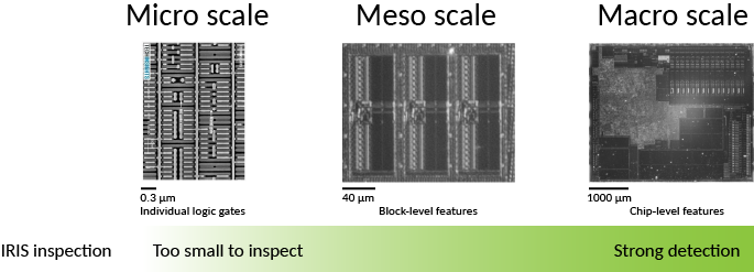
Above: Various size scales found on a chip, in relationship to IRIS capabilities.
IRIS cannot inspect the smallest features of a chip. The diagram above illustrates the various size scales found on a chip and relates it to the capabilities of IRIS. The three general feature ranges are prefixed with micro-, meso-, and macro-. On the left hand side, “micro-scale” features such as individual logic gates will be smaller than a micron tall. These are not resolvable with infra-red wavelengths and as such not directly inspectable via IRIS, so the representative image was created using SEM. The imaged region contains about 8 individual logic gates.
In the middle, we can see that “meso-scale” features can be constrained in size and identity. The representative image, taken with IRIS, shows three RAM “hard macros” in a 55 nm process. Individual row sense amplifiers are resolvable in this image. Even in a more modern sub-10 nm process, we can constrain a RAM’s size to plus/minus a few rows or columns.
On the right, “macro-scale” features are clearly enumerable. The number and count of major functional blocks such as I/O pads, data converters, oscillators, RAM, FLASH, and ROM blocks are readily identified.
IRIS is a major improvement over simply reading the numbers printed on the outside of a chip’s package and taking them at face value. It’s comparable to being able to X-ray every suitcase for dangerous objects, versus accepting suitcases based solely on their exterior size and shape.
Even with this improvement, malicious changes to chips – referred to as “hardware trojans” – can in theory remain devilishly difficult to detect, as demonstrated in “Stealthy Dopant-Level Hardware Trojans” by Becker, et al (2013). This paper proposes hardware trojans that only modulate the doping of transistors. Doping modifications would be invisible to most forms of inspection, including SEM, X-Ray ptychography, and IRIS.
The good news is that the attacks discussed (Becker, 2013) are against targets that are entirely unhardened against hardware trojans. With a reasonable amount of design-level hardening, we may be able to up the logic footprint for a hardware trojan into something large enough to be detected with IRIS. Fortunately, there is an existing body of research on hardening chips against trojans, using a variety of techniques including logic locking, built in self test (BIST) scans, path delay fingerprinting, and self-authentication methods; for an overview, see “Integrated Circuit Authentication” by Tehranipoor.
IRIS is a necessary complement to logic-level hardening methods, because logic-only methods are vulnerable to bypasses and emulation. In this scenario, a hardware trojan includes extra circuitry to evade detection by spoofing self-tests with correct answers, like a wolf carrying around a sheep’s costume that it dons only when a shepherd is nearby. Since IRIS can constrain meso-scale to macro-scale structure, we can rule out medium-to-large scale circuit modifications, giving us more confidence in the results of the micro-scale verification as reported by logic-level hardening methods.
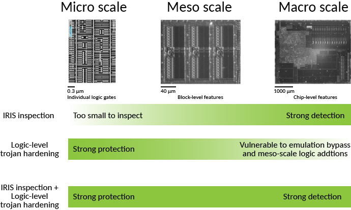
Above: Comparison of the detection-vs-protection trade offs of logic level hardening and IRIS inspection.
Thus, IRIS can be used in conjunction with logic-level trojan hardening to provide an overall high-confidence solution in a chip’s construction using non-destructive and in situ techniques, as illustrated above.
The primary requirement of the logic-level hardening method is that it must not be bypassable with a trivial amount of logic. For example, simple “logic locking” (a method of obfuscating logic which in its most basic form inserts X(N)ORs in logic paths, requiring a correct “key” to be applied to one input of the X(N)ORs to unlock proper operation) could be bypassed with just a few gates once the key is known, so this alone is not sufficient. However, a self-test mechanism that blends state from “normal runtime” mode and “self test” mode into a checksum of some sort could present a sufficiently high bar. In such a stateful verification mechanism, the amount of additional logic required to spoof a correct answer is proportional to the amount of state accumulated in the test. Thus, one can “scale up” the coverage of a logic-level test by including more state, until the point where any reliable bypass would be large enough to be detected by IRIS (thanks to jix for pointing me in the right direction!). The precise amount of state would depend on the process geometry: smaller process geometries would need more state.
Under the assumption that each extra bit would imply an additional flip flop plus a handful of gates, a back-of-the-envelope calculation indicates a 28 nm process would require just a few bits of state in the checksum. In this scenario, the additional trojan logic would modify several square microns of chip area, and materially change the scattering pattern of infra-red light off of the chip in the region of the modification. Additional techniques such as path delay fingerprinting may be necessary to force the trojan logic to be spatially clustered, so that the modification is confined to a single region, instead of diffused throughout the standard cell logic array.
Summary and Future Direction
IRIS is a promising technique for improving trust in hardware. With a bit of foresight and planning, designers can use IRIS in conjunction with logic hardening to gain comprehensive trust in a chip’s integrity from micro- to macro-scale. While the technique may not be suitable for every chip in a system, it fits comfortably within the parameters of chips requiring high assurance such as trust roots and secure enclaves.
Of course, IRIS is most effective when combined with open source chip design. In closed source chips, we don’t know what we’re looking at, or what we’re looking for; but with open source chips we can use the design source to augment the capabilities of IRIS to pinpoint features of interest.
That being said, I’m hoping that IR-capable microscopes become a staple on hardware hacker’s workbenches, so we can start to assemble databases of what chips should look like – be they open or closed source. Such a database can also find utility in everyday supply chain operations, helping to detect fake chips or silent die revisions prior to device assembly.
Over the coming year, I hope to improve the core IRIS technique. In addition to upgrading optics and adding image stitching to my toolbox, digitally controlling the angle and azimuth of incident light should play a significant role in enhancing the utility of IRIS. The sub-wavelength features on a chip interact with incident light like a hologram. By modifying the azimuth and angle of lighting, we can likely glean even more information about the structure of the underlying circuitry, even if they are smaller than the diffraction limit of the system.
A bit further down the road, I’d like to try combining IRIS with active laser probing techniques, where IRIS is used to precisely locate a spot that is then illuminated by an intense laser beam. While this has obvious applications in fault induction, it can also have applications in verification and chip readout. For example, the localized thermal stimulation of a laser can induce the Seeback effect, creating a data-dependent change in power consumption detectable with sensitive current monitors. I note here that if physical tamper-resistance is necessary, post-verification a chip can be sealed in opaque epoxy with bits of glitter sprinkled on top to shield it from direct optical manipulation attacks and evil-maid attacks. However, this is only necessary if these attacks are actually part of the threat model. Supply chain attacks happen, by definition, upstream of the end user’s location.
The other half of optical chip verification is an image processing problem. It’s one thing to have reference images of the chip, and it’s another thing to be able to take the image of a chip and compare it to the reference image and generate a confidence score in the construction of the chip. While I’m not an expert in image processing, I think it’s important to at least try and assemble a starter pipeline using well known image processing techniques. A turnkey feature extraction and comparison tool would go a long way toward making IRIS a practically useful tool.
Ultimately, the hope is to create a verification solution that grows in parallel with the open source chip design ecosystem, so that one day we can have chips we can trust. Not only will we know what chips are intended to do, we can rest assured knowing they were built as intended, too.
This research is partially funded by a NGI Zero Entrust grant from NLnet and the European Commission, as well as by the donations of Github Sponsors.


Thanks but, I will stick with towels and not blasting bacteria back onto my hands from the air.

1 public comment


I know hand dryers have their problems, but I think for fun we should keep egging Dyson on and see if we can get them to make one where the airflow breaks the speed of sound.


1 public comment
"30÷ off" is so wonderfully evil, I must use it everywhere possible
Silicon Valley, CA


2 public comments

As a medical librarian, I can confirm that this is a comic about health data.
ATL again
Next Page of Stories